Post Time:Oct 27,2016Classify:Industry NewsView:1260

This new method was born of a surprising phenomenon: irradiating glass in a particular way with an ultrafast laser has the effect of making the glass up to a thousand times more sensitive to subsequent wet chemical etching.
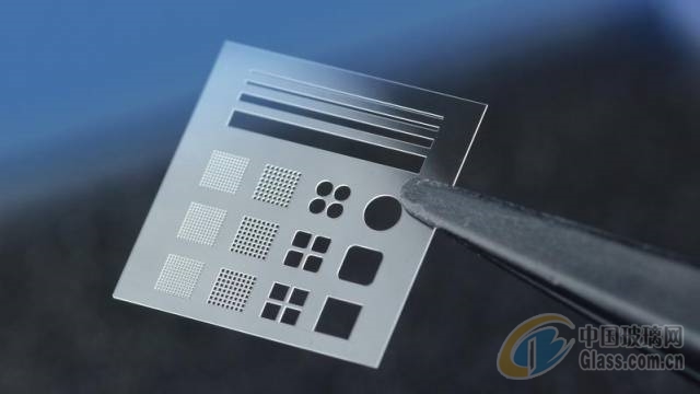
This means it is possible to guide a laser beam focused to a diameter of a few micrometers through a glass block and subsequently etch a fine tube through the volume of the glass. The method can be used to create the tiniest of holes, to etch complete microfluidic systems into the glass, or to make cuts with extremely high surface quality.
Results from Femto Digital Photonic Production Research Project
Before this phenomenon can be harnessed in industrial processes, there are still many questions to be answered. What are the interaction processes? Which materials are suitable? What are the optimum processing parameters? What type of processing technology is needed?
Answering these questions is the main aim of the BMBF-funded Femto Digital Photonic Production joint research project. Since 2014, representatives of three research chairs at RTWH Aachen University and of the Fraunhofer Institute for Laser Technology ILT have been collaborating with six companies to study new phenomena that arise when processing transparent materials with ultrafast laser pulses.
The researchers have developed a demonstrator in which different materials and processing parameters can be compared. The procedure dubbed selective laser etching (SLE) has been tested for several different types of glass materials, including quartz glass, sapphire, BOROFLOAT 33 and Corning Willow. Etch selectivities of 1000:1 between laser-structured and unstructured areas were reached in BOROFLOAT 33, and roughly 100:1 in Willow glass.
The next Step: Improving Process Understanding
In the next phase of the project, lasting until 2019, understanding of the process will be deepened. In this regard, several experiments will be conducted at the Chair for Laser Technology LLT at RWTH Aachen University, with complex simulations running in parallel at the Nonlinear Dynamics of Laser Manufacturing Processes Instruction and Research Department NLD. The Chair for Technology of Optical Systems TOS will concentrate on optimizing the optics in the systems.
Researchers are working to develop the process technology in collaboration with three laser source manufacturers (Amphos, Edgewave and TRUMPF) and three system suppliers (4Jet, LightFab and Pulsar Photonics). Their goal is to develop multiple beam systems for large surface use as well as smaller systems for micro-processing.
LightFab GmbH, a start-up from former employees from the Chair of Laser Technology at the RWTH Aachen University, uses Selective Laser-induced Etching (SLE) to produce 3D precision parts made of quartz glass. Their machine that does this – the LightFab 3D Printer – was honored with the Prism Award at Photonics West 2016. This machine increases the productivity of the subtractive 3D printing of glass components for prototypes and series and, thanks to its high-speed modules, makes it possible to mass produce components with the SLE process.
Potential Applications from Biomedicine to Electronics
Already the project partners can see a multitude of potential applications for the technique. For microfluidics, it can produce not only channels in glass materials but also nozzles and other micro-components.
The technique also offers substantial advantages in drilling and cutting processes. Etching allows tension-free material ablation, which is advantageous for instance when manufacturing interposer structures in semiconductor technology. It can produce structures measuring under 10 μm. Meanwhile, new systems with high laser power and multi-beam optics hold major potential for reaching a high throughput.
Source: www.glassonline.comAuthor: shangyi